Core concepts
Cells, geometry, ports, and placement handles describe the design. Bookmarks and Notes add application metadata.
| Noun | What it is |
|---|---|
LayerSpec |
A (layer, datatype) pair, optionally with design rules. |
Layer |
A LayerSpec carrying min-width / min-spacing / min-radius. |
| Cell | A reusable hierarchical block, built with lm.CELL. |
| Port | A named connection point on a cell. |
| Bookmark | A named bbox bookmark - surfaces in the viewer’s Bookmarks tab. |
| Note | User-authored information for Lumicron Notebook. |
| Verb | What it does |
|---|---|
add |
Adds a shape, port, bookmark, sub-cell, or array to a cell. |
Place |
Locates an added thing - chained with at, move_by, rotate_by. |
Route |
Connects two ports - auto by default, manual via .go(). |
Naming convention
The library uses three case styles to make intent visible at a glance:
- ALL CAPS for language primitives:
CELL,ARRAY,PORT. - PascalCase for shapes, components, and PDK objects:
Rectangle,Ring,Waveguide,Pad. - lowercase for chain methods:
.at(),.go(),.style(),.add_bookmark(); directional flips are.flipX()and.flipY().
Once you’ve seen this once, scripts read like English sentences.
Layers
A layer is a (layer_number, datatype) pair. You can allocate one by hand:
metal = lm.LayerSpec(layer=4, datatype=0)
silicon = lm.LayerSpec(layer=9, datatype=0)
…or pull them from a PDK module, where they come pre-named with design rules attached:
"""Using a PDK's predefined layers and design rules.

Instead of allocating layer numbers by hand, import a PDK module and
read the named layers from its `LAYER` namespace. Each entry is a
`Layer` (subclass of `LayerSpec`) carrying min-width, min-spacing, and
min-radius rules — the router and tapers consult those automatically.
"""
import lumicron as lm
import lumicron.pdks.elyon_demo.all as pdk


@lm.pcell
def PDKLayers():
    c = lm.CELL("PDKLayers")

    # Silicon waveguide-width strip on the SILC layer.
    strip = lm.Rectangle(x_dim=200, y_dim=0.5, layer=pdk.LAYER.SILC)
    c.add(strip)
    c.Place(strip).at((0, 0))

    # Silicon nitride strip, twice as wide, sitting above.
    siln = lm.Rectangle(x_dim=200, y_dim=1.0, layer=pdk.LAYER.SILN)
    c.add(siln)
    c.Place(siln).at((0, 20))

    # Metal-1 pad.
    pad = lm.Rectangle(x_dim=80, y_dim=80, layer=pdk.LAYER.MTL1)
    c.add(pad)
    c.Place(pad).at((250, 0))
    return c


if __name__ == "__main__":
    PDKLayers().to_gds("pdk_layers.gds")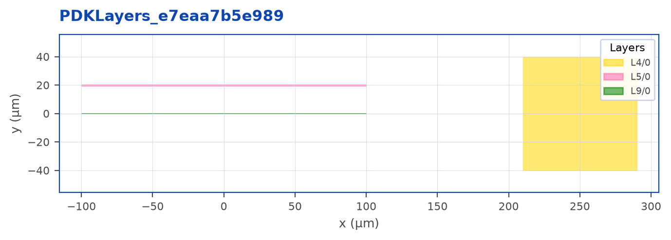
Tip
A PDK’s layers are not just numbers - they’re Layer objects carrying min_width, min_spacing, and min_radius. The router applies the resolved minimum-radius rule to rendered curvature. A declared Euler layout radius is not itself a minimum-curvature guarantee.
Cells
A cell is a named container. It can hold:
- Shapes (
Rectangle,Polygon,Circle,Ring, …) - Sub-cells (other
CELLs, including from a PDK) - Arrays (
ARRAYof a child cell on a regular grid) - Ports (
PORT- labeled connection points) - Bookmarks (
Bookmark- labeled fit-to-screen bookmarks)
chip = lm.CELL("MyChip")
chip.add(lm.Rectangle(x_dim=100, y_dim=50, layer=metal))
c.add(...) returns a handle. Pass it to c.Place() to position that object. Sub-cell handles expose handle.ports["o1"]. Compact array occurrences expose geometry and bounds, not ports; use individual placements when each component needs a connection. For shapes you can pass either the original object or the handle to Place(); both work. Metadata additions return no geometry handle.
Ports
A port marks a directional connection point: a position, an angle, a width, and the layer it lives on.
chip.add(lm.PORT(
    "in", position=(0, 0), direction=0,
    width=0.5, layer=pdk.LAYER.SILC,
))directionis degrees CCW from +X (0 = East, 90 = North, 180 = West, 270 = South).port_typedefaults to"optical". Passport_type="electrical"for a metal pad’s port.route_profile=(optional) attaches a cross-section recipe - see Chapter 5.
Access ports on a cell via c.ports["name"]; on a child handle via handle.ports["name"].
Inspection and physical export
Keep the CELL as the authoring object. Lumicron Run discovers top-level cells; standalone scripts can export explicitly:
print(chip.inspect())
info = chip.inspect(as_dict=True)
chip.to_gds("chip.gds")
chip.to_oas("chip.oas")
netlist = chip.extract_netlist()
inspect() resolves a snapshot and reports definition-local objects, ports, bounds, route lengths with their measurement method and coverage, and custom data. It does not infer a path length from arbitrary polygons or certify fabrication/connectivity. The extracted netlist is a result, not an LVS pass.
to_gds() defaults to max_points=0 (unlimited vertices). Use max_points=199 only when the submission rules require legacy GDS limits. .lum persistence is owned by the application; there is no generic Script save() or export() verb. Internal Layout/compiler models are not designer-root constructors.
Cell information
Use add_info() for information your team wants to keep with a cell definition:
chip.add_info({"owner": "Photonics Team", "banana": 47,
               "path_length_um": 2345.67})
info = chip.inspect(as_dict=True)
print(info["cells"][chip.name]["user_info"])
Keys have no reserved meaning. path_length_um is your supplied value; it does not change a route length, DRC result or simulation. Repeated calls replace matching keys and retain other keys. Nested values are copied. Every placement of the definition shares its information; the method does not annotate individual instances. Existing add_data() remains available for its prior consumers.
Values may be strings, booleans, None, finite floats, integers from -(2**53 - 1) to 2**53 - 1, lists, and dictionaries with string keys, nested up to 32 levels. Unsupported values raise before changing the definition. The integer range supports exact exchange with the native application’s JSON representation. Tuples, arbitrary objects, NaN and infinity are not converted.
Inspection keeps three separate per-cell records: user_info for these values, gds_metadata for original imported artifact records, and lumicron_info for bounded structural evidence. The Inspector uses the corresponding User Information, GDS Metadata, and Lumicron Information sections.
CellFromGDS retains source properties (including property bytes), labels, references and native PATH spines as inert source records. Their frame is the original source definition, even though the imported physical cell contains flattened polygons. A stored PATH’s vertex-chain length excludes end extensions; it is not an optical length for the whole cell or a measurement of later edits. Polygon-only cells remain unresolved. None of this supplies Route.length.
Layout snapshots, .lum semantic records, and digest-matched GDS sidecars retain this information. Raw GDS and OAS exports carry physical geometry, not arbitrary user information. Importing a GDS without its matching sidecar cannot recover those user values. Selecting an individual exported definition recovers its information; flattening a parent does not promote each child’s annotations onto that parent. Existing OAS viewer/geometry support does not imply a new CellFromGDS OAS authoring contract.
Package ownership
Design with import lumicron as lm. Author fabrication platforms with import lumicron_pdk as lpdk; write custom DRC/DFX libraries with import lumicron_validate as lv. These are separate public interfaces. The old lumicron_api namespace is a deprecated compatibility bridge.
Physical-simulation and experimental Script/Schematic APIs are archived, with internal application integrations retained. This guide does not prescribe their future replacement. XOR comparison is not a canonical Script primitive.