Components
Components are the named building blocks your PDK exposes - pads, edge couplers, MMIs, modulators, photodiodes. Each is a @pcell-decorated function that returns a CELL. End users instantiate them like functions; the decorator records definition identity, parameters, and cell naming.
A simple component
"""A simple PDK component with @pcell.

The `@pcell` decorator turns a function into a parametrized cell
factory. Each unique combination of non-default arguments yields a
distinct cell name automatically — distinct calls don't collide in GDS,
identical calls share the same cell definition under the hood.
"""
import lumicron as lm
import lumicron_pdk as lpdk

LAYER = lpdk.LayerTable(
    MTL1 = lpdk.Layer(4, 0, color="#ffd700", min_width=1.0, min_spacing=1.0),
)


@lm.pcell
def Pad(size: float = 80.0, layer: lm.LayerSpec = LAYER.MTL1):
    """A square electrical bond pad with one electrical port."""
    c = lm.CELL("Pad")

    body = lm.Rectangle(x_dim=size, y_dim=size, layer=layer)
    h = c.add(body)
    c.Place(h).at((0, 0))

    # Publish a port at the south edge so routes can land on it.
    c.add(lm.PORT(
        "p", position=(0, -size / 2), direction=270,
        width=size, layer=layer, port_type="electrical",
    ))
    return c


@lm.pcell
def PadDemo():
    """Two pads side-by-side at different sizes — different cell names auto-derived."""
    c = lm.CELL("PadDemo")
    p1 = c.add(Pad(size=80))
    p2 = c.add(Pad(size=120))
    c.Place(p1).at((0, 0))
    c.Place(p2).at((250, 0))
    return c


if __name__ == "__main__":
    PadDemo().to_gds("pad_demo.gds")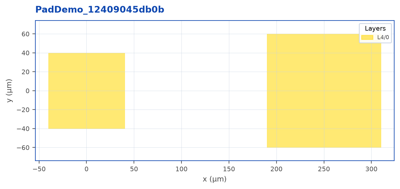
What @pcell is doing for you:
- Stable identity. The name is derived from the qualified factory, source, PDK identity, and effective typed parameters, including defaults. Imported GDS content also contributes to identity.
- Fresh construction. Each call executes the factory and returns its constructed cell. Repeated calls are not a cache of the same mutable
CELLobject. To reuse one constructed definition, keep that cell and add it to the parent more than once.
This is the same shape as IPKISS PCells or KFactory cells - if you know one, you know this.
Publishing ports with route profiles attached
This is the workflow that makes a polished PDK. Every port your component publishes carries a route_profile= so end-user routes off it inherit the cross-section automatically.
"""A component publishing ports with an attached route profile.

The trick that makes a well-curated PDK feel effortless: every
component publishes ports that already know their cross-section. End
users call ``c.Route(a.ports["o1"], b.ports["i1"])`` with no kwargs and
the route automatically stamps the right layers, claddings, and
periodic features.
"""
import lumicron as lm
import lumicron_pdk as lpdk

LAYER = lpdk.LayerTable(
    SILC = lpdk.Layer(9, 0, color="#008000", min_width=0.2, min_radius=5.0),
    OXID = lpdk.Layer(1, 0, color="#87ceeb"),
)


@lpdk.route_profile(port_width=0.5, radius=10.0, radius_min=5.0)
def silc_strip(p):
    p.layer(LAYER.SILC, width=p.port_width)
    p.layer(LAYER.OXID, width=p.port_width + 4.0)


@lm.pcell
def EdgeCouplerSi(length: float = 100.0, tip_width: float = 0.1):
    """A linear taper from a 0.1 µm tip to a 0.5 µm body, with an
    OXID cladding region around it. The output port carries
    `silc_strip` so any route off it inherits the profile."""
    c = lm.CELL("EdgeCouplerSi")

    # The taper polygon: tip → body, 4 vertices.
    body_w = 0.5
    taper = lm.Polygon(
        vertices=[
            (0, -tip_width / 2),
            (length, -body_w / 2),
            (length, body_w / 2),
            (0, tip_width / 2),
        ],
        layer=LAYER.SILC,
    )
    c.add(taper)
    c.Place(taper).at((0, 0))

    # OXID cladding rectangle hugging the taper.
    clad = lm.Rectangle(x_dim=length, y_dim=body_w + 4, layer=LAYER.OXID)
    h = c.add(clad)
    c.Place(h).using("SW").at((0, -(body_w + 4) / 2))

    # Tip port (incoming from chip edge) and body port (publishes profile).
    c.add(lm.PORT("o_tip", position=(0, 0), direction=180,
                  width=tip_width, layer=LAYER.SILC))
    c.add(lm.PORT("o1", position=(length, 0), direction=0,
                  width=body_w, route_profile=silc_strip))
    return c


@lm.pcell
def CouplerDemo():
    c = lm.CELL("CouplerDemo")
    cpl = c.add(EdgeCouplerSi(length=100))
    c.Place(cpl).at((0, 0))

    # Publish a destination port on the chip and route from coupler.o1.
    # No `radius=` / `profile=` — both come from the port's profile.
    c.add(lm.PORT("out", position=(500, 100), direction=180,
                  route_profile=silc_strip))
    c.Route(cpl.ports["o1"], c.ports["out"])
    return c


if __name__ == "__main__":
    CouplerDemo().to_gds("coupler_demo.gds")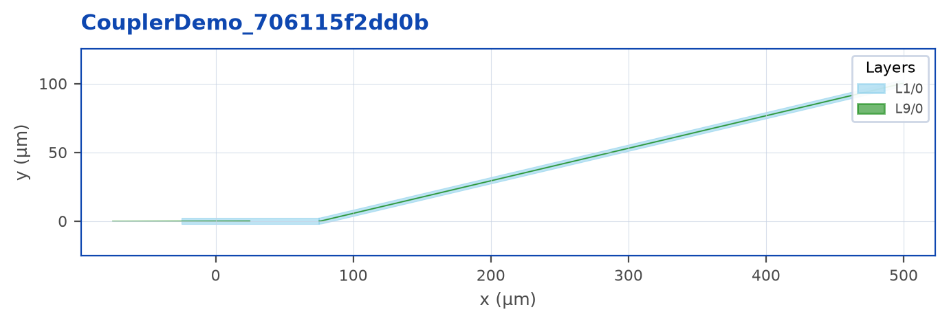
The relevant lines:
c.add(lm.PORT("o1", position=(length, 0), direction=0,
              width=body_w, route_profile=silc_strip))
Then in the end-user demo at the bottom:
chip.Route(cpl.ports["o1"], chip.ports["out"])No radius=, no profile= - the route inherits both from the port. The user’s script reads like a circuit diagram instead of a parameter dump.
What “good ports” look like
Three rules of thumb for component port design:
Use the same port-name convention everywhere. i1/o1 for two-port elements, i1, o1, o2 for splitters, o_tip for edge-coupler facet ports. Once an end user has learned your convention, they shouldn’t have to consult docs to route between any two of your components.
Direction matters. Optical ports point outward from the cell - direction=0 (East) for a port on the right edge, 180 (West) for the left, 90 for the top, 270 for the bottom. The router uses port direction to pick Manhattan vs direct routing.
Always attach a route profile. If a port is on a layer your PDK has no profile for, add a profile for it. The cost of an extra profile is one decorated function; the payoff is end-user scripts that route through your component without thinking.
Synthesizing geometry
Inside the component body, you have the full lumicron toolkit:
| Tool | When to use it |
|---|---|
lm.Rectangle(x_dim, y_dim, layer) |
Square / rectangular regions, pads, body slabs. |
lm.Polygon(vertices=[…], layer) |
Tapers, spline-like profiles, anything non-rectangular. |
lm.Ring(outer_radius, width, layer) |
Ring resonators, annular regions. |
lm.Circle(radius, layer) |
Filled circles - alignment marks, photonic-crystal holes. |
lm.ARRAY(child, count, pitch) |
Periodic features - via arrays, contact arrays. |
lm.Waveguide(points, layer, width, …) |
Tapered curvy paths (S-bends in components, spirals). |
c.add(child_cell) + c.Place(...) |
Hierarchical sub-components. |
Promoting child ports
When a component contains sub-cells whose ports you want to expose as the component’s own:
@lm.pcell
def MZI(length: float = 200, width: float = 0.5):
    c = lm.CELL("MZI")
    splitter = c.add(YSplitter(width=width))
    combiner = c.add(YSplitter(width=width))
    c.Place(splitter).at((0, 0))
    c.Place(combiner).at((length + 60, 0)).rotate_by(180)

    # Re-publish splitter's input as MZI's input.
    splitter.promote(ports=["i1"])
    # Re-publish combiner's input as MZI's output, with a renamed key.
    combiner.promote(ports={"i1": "o1"})

    return c
handle.promote() accepts a list of names, a rename dict, or None (everything). An optional prefix= namespaces them when multiple children expose ports of the same name.
Packaged schematic and model metadata
The existing packager preserves declared symbol hints and named compact-model metadata in legacy/application integrations. Review any port_resolution_error or model_resolution_error before publishing. Geometry alone does not supply a circuit model. Experimental CELL.Model/CELL.Simulate syntax is archived; this guide does not teach it as a future public simulation API. Existing packaged models remain readable through deprecated compatibility forwarding.
Component design patterns
Sensible defaults beat exhaustive parameters. Pick sensible foundry-typical defaults for everything; expose the kwargs that real users will actually want to vary. A modulator with 30 parameters is hard to use; one with 5 parameters and good defaults is easy.
Match the foundry datasheet’s parameter names. If the foundry’s PDK calls it arm_length, name your kwarg arm_length. End users cross-reference the datasheet while writing scripts.
Validate inputs early. Raise ValueError with a useful message when a parameter is out of range. Better to fail at component construction than at GDS-write time.
Set the cell name from a static string + the decorator handles the rest. Use a readable lm.CELL("ComponentName") inside the factory; @pcell derives the final bounded name from the factory name and definition identity. Don’t try to compose the full name yourself.
Tip
A useful trick when porting an existing PDK: write each component’s tests first, expressing what end-user scripts should look like (Pad(size=80).ports["p"], MZI(length=200).ports["i1"]). Then implement the components to make the tests pass. The result is a PDK whose API was designed from the user’s seat.