Cookbook - a minimal PDK from scratch
Everything in one file. Layers, profiles, components, transitions. In a real distribution each chunk lives in its own module; here it’s collapsed so you can see the whole thing at once.
"""A complete, single-file minimal PDK.

In a real distribution, layers / profiles / components / transitions
each live in their own module. For learning purposes everything is
collapsed into one file here. The end-user import surface is the same:

    import lumicron.pdks.tinyphot.all as pdk
    pdk.LAYER.SILC
    pdk.RP.silc_strip
    pdk.Pad(size=80)
"""
import lumicron as lm
import lumicron_pdk as lpdk

# ── Layers ───────────────────────────────────────────────────
LAYER = lpdk.LayerTable(
    SILC = lpdk.Layer(9, 0, color="#008000", min_width=0.2, min_radius=5.0),
    SILN = lpdk.Layer(5, 0, color="#ff69b4", min_width=0.4, min_radius=10.0),
    OXID = lpdk.Layer(1, 0, color="#87ceeb"),
    MTL1 = lpdk.Layer(4, 0, color="#ffd700", min_width=1.0, min_spacing=1.0),
)

# ── Route profiles ───────────────────────────────────────────
@lpdk.route_profile(port_width=0.5, radius=10.0, radius_min=5.0)
def silc_strip(p):
    p.layer(LAYER.SILC, width=p.port_width)
    p.layer(LAYER.OXID, width=p.port_width + 4.0)


@lpdk.route_profile(port_width=0.5, radius=10.0, radius_min=5.0)
def siln_strip(p):
    p.layer(LAYER.SILN, width=p.port_width)
    p.layer(LAYER.OXID, width=p.port_width + 4.0)


RP = lpdk.RouteProfiles(silc_strip=silc_strip, siln_strip=siln_strip)


# ── Components ───────────────────────────────────────────────
@lm.pcell
def Pad(size: float = 80.0):
    c = lm.CELL("Pad")
    body = lm.Rectangle(x_dim=size, y_dim=size, layer=LAYER.MTL1)
    h = c.add(body)
    c.Place(h).at((0, 0))
    c.add(lm.PORT("p", position=(0, -size / 2), direction=270,
                  width=size, layer=LAYER.MTL1, port_type="electrical"))
    return c


@lm.pcell
def Waveguide(length: float = 100.0):
    """A straight waveguide stub — useful for grating couplers, taps."""
    c = lm.CELL("Waveguide")
    rect = lm.Rectangle(x_dim=length, y_dim=0.5, layer=LAYER.SILC)
    h = c.add(rect)
    c.Place(h).using("SW").at((0, -0.25))
    c.add(lm.PORT("o1", position=(0, 0), direction=180,
                  width=0.5, route_profile=silc_strip))
    c.add(lm.PORT("o2", position=(length, 0), direction=0,
                  width=0.5, route_profile=silc_strip))
    return c


# ── Transitions ──────────────────────────────────────────────
def silc_siln_elevator():
    return lpdk.PhotonicElevator(
        layer_a=LAYER.SILC, layer_b=LAYER.SILN,
        width_a=0.5, width_b=0.5,
        tip_a=0.08, tip_b=0.08,
        taper_length_a=25.0, taper_length_b=25.0,
        overlap=10.0,
        cladding_layer=LAYER.OXID, cladding_margin=2.0,
        route_profile_a=silc_strip,
        route_profile_b=siln_strip,
    )


TRANSITIONS = lpdk.TransitionRegistry()
TRANSITIONS.register(LAYER.SILC, LAYER.SILN, silc_siln_elevator)
lpdk.default_transitions().register(LAYER.SILC, LAYER.SILN, silc_siln_elevator)


# ── Demo cell using the PDK we just defined ──────────────────
@lm.pcell
def TinyPhotDemo():
    c = lm.CELL("TinyPhotDemo")
    wg1 = c.add(Waveguide(length=80))
    wg2 = c.add(Waveguide(length=80))
    c.Place(wg1).at((0, 0))
    c.Place(wg2).at((300, 200)).rotate_by(180)
    c.Route(wg1.ports["o2"], wg2.ports["o2"])
    return c


if __name__ == "__main__":
    TinyPhotDemo().to_gds("tinyphot_demo.gds")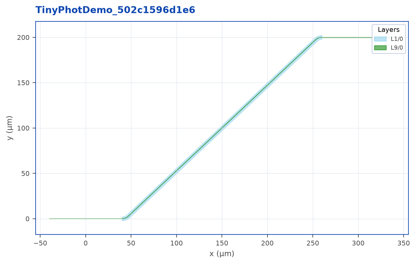
Splitting it into a package
To turn this single file into the distributable layout from Chapter 1, copy each section into its own module:
tinyphot/layers.py-
LAYERandSTACKdefinitions. Imports onlylumicron. tinyphot/profiles.py-
silc_strip,siln_strip,RP. ImportsLAYERfrom.layers. tinyphot/components.py-
Pad,Waveguide. ImportsLAYERand the route profiles. tinyphot/transitions.py-
silc_siln_elevator(),TRANSITIONS, thedefault_transitions().register(...)call. ImportsLAYERandRP. tinyphot/__init__.py- Re-exports the four names.
tinyphot/all.py-
from .layers import LAYER, STACK from .profiles import RP from .transitions import TRANSITIONS from .components import * # noqa tinyphot/meta.py-
META = {
    "name": "TinyPhot Research PDK",
    "package-name": "tinyphot",
    "version": "0.1.0",
}
That’s the conventional shape end users see. The same package source ships in your PyPI wheel; lumicron_pdk.packaging writes the package’s Python files at the .lumpdk archive root, and the app materializes them in a private cache for the active project. Relative imports keep the package usable in both environments.
What this minimal PDK is missing
A production-grade PDK has more than this:
- More components. Edge couplers, MMIs, modulators, photodiodes, ring resonators with thermal heaters, contact arrays.
- More profiles. A rib profile, a slot-mode profile, a periodic-cladding sub-wavelength profile, an electrical profile.
- More transitions. SILC-to-MTL1 ohmic contact, SILN-to-III-V wafer bond.
- A proper
LayerStackwith Sellmeier coefficients. This minimal stack would not power a usable mode solver. - Test scripts.
test_pad.py,test_components_smoke.py. - Documentation. README with tested examples, component docstrings, and foundry constraints.
You add these as you go - start with the four-section shape and grow the package.
Verifying it works
Drop the file at tinyphot/__init__.py (alongside lumicron’s package directory in your environment, or anywhere on PYTHONPATH), then:
python -c "
import lumicron as lm
import tinyphot as pdk

chip = lm.CELL('Smoke')
wg = chip.add(pdk.Waveguide(length=200))
chip.Place(wg).at((0, 0))
chip.to_gds('smoke.gds')
"
If smoke.gds lands and contains a SILC strip 200 µm long, your PDK is wired up. From there, it’s a matter of growing the component library and refining the rules.