The physical stack
The LayerStack records authored layer thicknesses, vertical positions, and optical material data. Lumicron packages these declarations for technology inspection and simulation consumers. A stack declaration alone does not run a field solver; Maple execution remains disabled in this alpha.
If your PDK doesn’t have public stack data (e.g. NDA’d foundry process), you can ship the layer table only and add the stack later. Components and routing don’t depend on it.
A complete stack
"""A physical layer stack with Sellmeier dispersion.

The `LayerStack` describes the physical reality of the process — what
sits on what, how thick each layer is, and the material's dispersive
refractive index. Simulators (mode solvers, FDTD wrappers) read the
stack to set up their cross-section.
"""
import lumicron as lm
import lumicron_pdk as lpdk

LAYER = lpdk.LayerTable(
    BOX  = lpdk.Layer(1, 0, color="#87ceeb"),
    SILC = lpdk.Layer(9, 0, color="#008000", min_width=0.2,
                    min_spacing=0.2, min_radius=5.0),
    SILN = lpdk.Layer(5, 0, color="#ff69b4", min_width=0.4,
                    min_spacing=0.3, min_radius=10.0),
    CLAD = lpdk.Layer(2, 0, color="#aac7e8"),
    MTL1 = lpdk.Layer(4, 0, color="#ffd700"),
)

# Sellmeier coefficients describe n(λ) for a material. The form is
# n²(λ) − 1 = Σ B_i · λ² / (λ² − C_i).
SiO2 = lpdk.Sellmeier(
    B=[0.6962, 0.4079, 0.8975],
    C=[0.0684**2, 0.1162**2, 9.8962**2],
)
Si = lpdk.Sellmeier(
    B=[10.6684, 0.0030, 1.5413],
    C=[0.3015**2, 1.1348**2, 1104.0**2],
)
SiN = lpdk.Sellmeier(B=[2.8939], C=[0.1397**2])

STACK = lpdk.LayerStack(
    lpdk.StackLayer("BOX",      layer=LAYER.BOX,  thickness=2.0,  sellmeier=SiO2),
    lpdk.StackLayer("core_si",  layer=LAYER.SILC, thickness=0.22, sellmeier=Si),
    lpdk.StackLayer("core_sin", layer=LAYER.SILN, thickness=0.4,  sellmeier=SiN),
    lpdk.StackLayer("clad",     layer=LAYER.CLAD, thickness=2.0,  sellmeier=SiO2),
    lpdk.StackLayer("metal1",   layer=LAYER.MTL1, thickness=1.0,  n=0.0),
)


@lm.pcell
def StackPreview():
    """A layout that exposes the stack's process layers as a strip."""
    c = lm.CELL("StackPreview")
    for i, name in enumerate(["BOX", "SILC", "SILN", "CLAD", "MTL1"]):
        rect = lm.Rectangle(x_dim=80, y_dim=20, layer=getattr(LAYER, name))
        h = c.add(rect)
        c.Place(h).at((0, i * 30))
    return c


if __name__ == "__main__":
    StackPreview().to_gds("stack_preview.gds")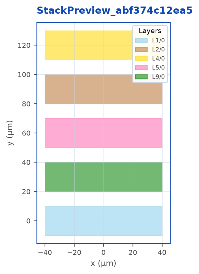
The material and stack building blocks:
| Type | Purpose |
|---|---|
Sellmeier |
Coefficients for n²(λ) = 1 + Σ B_i · λ² / (λ² − C_i). |
TabulatedIndex |
Validated wavelength samples; use bulk material data for a stack layer. |
StackLayer |
One physical layer: name, GDS layer ref, thickness, optical model. |
LayerStack |
Ordered collection of StackLayers, bottom to top. |
Sellmeier coefficients
The Sellmeier equation is the standard way to express dispersive n(λ) for transparent dielectrics. lumicron.Sellmeier(B=[…], C=[…]) takes the textbook coefficients in Bᵢ / λ²-units. SiO2, Si, and SiN have well-known constants - copy them from a reference (Palik, Malitson, IUPAC) so your end users get accurate dispersion.
For a declared constant real index approximation, pass n= directly:
lpdk.StackLayer("cladding", layer=LAYER.OXID, thickness=1.0, n=1.44)Use only one of n, sellmeier, or tabulated on each layer. tabulated must describe a bulk material, not a waveguide effective index. If optical properties are unavailable, leave them unspecified; n=0 is not a special declaration of a metal or perfect conductor.
Layer order
When z_start is omitted, the first layer starts at zero and each following layer starts at the preceding layer’s end. An explicit z_start is preserved, including zero or negative positions, and can express a gap or overlap. z_min and z_max report the resulting stack envelope. A typical authored SOI sequence might be:
- BOX (buried oxide)
- Silicon waveguide core
- (optional) silicon nitride strip
- Top oxide cladding
- Metal-1
- Inter-metal oxide
- Metal-2
Match your foundry’s PDK datasheet exactly. Off-by-one errors here are subtle - they don’t break compilation, just mode-solver results.
When the stack matters at runtime
Routing geometry is declared by profiles and components; the stack provides separate physical technology metadata. It is serialized into the PDK manifest and available through pdk.STACK. Use pdk.STACK.print_stack(), iterate its layers, or inspect a named layer’s thickness, z_start, and n_at(wavelength) value. A LayerStack.cross_section(at=...) method is not part of the current API.
Publish only material and dimensional values supported by your process data. Missing optical data should remain missing, rather than being filled with a placeholder that could be mistaken for a validated simulation input.
Note
The stack does not describe processing steps (e.g. “after litho on SILC, etch is partial”). It’s a finished-process model. Process-history modeling, when it matters (TCAD-style flows), lives outside the PDK in tooling that consumes the stack as a starting point.