Route profiles
A route profile is the cross-section recipe a router consults when it stamps a waveguide. It describes:
- One or more continuous strokes - the core, the claddings, exclusion zones, slot rails - each at a given width and offset.
- Optionally, periodic features - grating teeth, periodic claddings, electrical stitching - laid down at a fixed period along the route.
Once a profile exists, end users stop thinking about per-stroke geometry. They attach the profile to a port; every route off that port inherits it. This chapter is the most important one in this guide because attaching profiles to component ports is the single biggest UX investment a PDK author makes.
The decorator
import lumicron as lm
import lumicron_pdk as lpdk

@lpdk.route_profile(port_width=0.5, radius=10.0, radius_min=5.0)
def my_profile(p):
    p.layer(LAYER.SILC, width=p.port_width)
Decorator settings:
| Kwarg | Purpose |
|---|---|
port_width |
Default PORT.width when callers don’t override. Available as p.port_width inside the body. |
radius |
Default bend radius. Routes inherit it unless they pass an explicit radius=. |
radius_min |
Required minimum rendered curvature radius, distinct from the layout footprint. Defaults to radius. |
port_layer |
Optional fallback for PORT.layer. Defaults to the first layer declared in the body. |
name |
Optional explicit name. Defaults to the function name. |
The decorator returns a RouteProfile object. Pass it as route_profile= on a PORT(...) call, or as profile= on a Route(...) call.
A minimal profile - single core
"""A minimal route profile — single core stroke.

The `@lpdk.route_profile` decorator turns a builder function into a
RouteProfile. Inside the body, call `p.layer(...)` once per continuous
stroke. The profile here defines just the silicon core — no claddings.
"""
import lumicron as lm
import lumicron_pdk as lpdk

LAYER = lpdk.LayerTable(
    SILC = lpdk.Layer(9, 0, color="#008000", min_width=0.2, min_radius=5.0),
)


@lpdk.route_profile(port_width=0.5, radius=10.0, radius_min=5.0)
def silc_strip(p):
    """0.5 µm silicon core — minimal viable strip waveguide."""
    p.layer(LAYER.SILC, width=p.port_width)


# Optional: collect every profile this PDK exposes into one namespace,
# the way end-users will reference them as `pdk.RP.silc_strip`.
RP = lpdk.RouteProfiles(silc_strip=silc_strip)


@lm.pcell
def BasicProfileDemo():
    """Demo: route between two ports using the profile we just defined."""
    c = lm.CELL("BasicProfileDemo")
    c.add(lm.PORT(
        "in", position=(0, 0), direction=0,
        route_profile=silc_strip,
    ))
    c.add(lm.PORT(
        "out", position=(400, 200), direction=180,
        route_profile=silc_strip,
    ))
    c.Route(c.ports["in"], c.ports["out"])
    return c


if __name__ == "__main__":
    BasicProfileDemo().to_gds("basic_profile_demo.gds")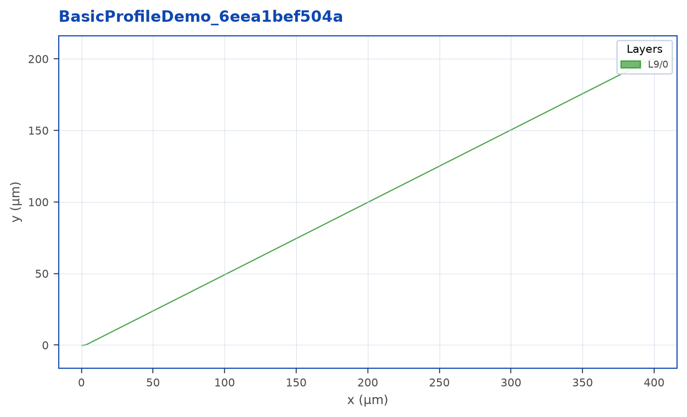
That’s a complete, usable profile. The route picks up its layer from p.layer(...), its width from p.port_width, and its bend radius from the decorator’s radius=.
Continuous strokes - p.layer()
p.layer(layer, *, width, offset=0.0)Each call adds one parallel band. offset is perpendicular to the centerline (positive = left of travel direction). Common patterns:
# Symmetric cladding (claddings auto-center on the stroke).
p.layer(LAYER.OXID, width=p.port_width + 4.0)

# Slot-mode rail - second stroke on the SAME layer, offset.
p.layer(LAYER.SILC, width=0.2, offset=+0.6)
p.layer(LAYER.SILC, width=0.2, offset=-0.6)

# Dopant rail running parallel.
p.layer(LAYER.NDOP, width=2.0, offset=+1.5)
A working cladded profile:
"""A cladded route profile — core + symmetric oxide cladding.

`p.layer()` can be called any number of times. Each call adds one
parallel stroke to the cross-section. Use it for claddings, exclusion
zones, slot-mode rails, or any sibling band that should run alongside
the core.
"""
import lumicron as lm
import lumicron_pdk as lpdk

LAYER = lpdk.LayerTable(
    SILC = lpdk.Layer(9, 0, color="#008000", min_width=0.2, min_radius=5.0),
    OXID = lpdk.Layer(1, 0, color="#87ceeb"),
)


@lpdk.route_profile(port_width=0.5, radius=10.0, radius_min=5.0)
def silc_cladded(p):
    """Silicon core with a 4 µm oxide cladding on either side."""
    p.layer(LAYER.SILC, width=p.port_width)
    p.layer(LAYER.OXID, width=p.port_width + 4.0)


@lm.pcell
def CladdedProfileDemo():
    c = lm.CELL("CladdedProfileDemo")
    c.add(lm.PORT(
        "in", position=(0, 0), direction=0,
        route_profile=silc_cladded,
    ))
    c.add(lm.PORT(
        "out", position=(400, 200), direction=180,
        route_profile=silc_cladded,
    ))
    c.Route(c.ports["in"], c.ports["out"])
    return c


if __name__ == "__main__":
    CladdedProfileDemo().to_gds("cladded_profile_demo.gds")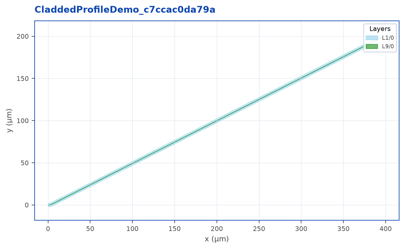
The router emits one FlexRoute per stroke. Bends share the same centerline, so widths and offsets stay consistent through corners.
Scalar PORTs and multistroke profiles
PORT.width is one scalar width in micrometres. It is not a list of rail apertures, a slot gap, or the full envelope of a multistroke cross-section. PORT(route_profile=profile) defaults to profile.port_width and profile.port_layer; explicit width= and layer= override those defaults. The connection-layer declaration is named port_layer, not connection_layer.
For routing, a centered stroke on port_layer is selected as primary, even when another layer was declared first. Its width follows the incoming scalar PORT width. If no such centered stroke exists, the first stroke remains primary and keeps its declared offset and width. Other strokes retain their own widths and offsets. Waveguide’s generated PORTs use that primary stroke’s width and layer; an explicitly constructed PORT still uses its own defaults.
Generic endpoint tapers compare each endpoint’s scalar width with the primary route width. They are centered linear polygons on the primary layer; they do not synthesize a transition for two separated rails. For example, declaring a 0.2 µm gap as port_width while the primary rail is 0.25 µm causes generic tapers under the default policy. RoutingPolicy(auto_taper=False) rejects that mismatch instead of changing the rails.
A bounded constant-rail pattern separates the gap from the scalar width:
@lpdk.route_profile(port_layer=LAYER.SILC, port_width=0.25,
                   routing_policy=lpdk.RoutingPolicy(auto_taper=False))
def fixed_slot(p):
    rail, gap = 0.25, 0.2
    p.layer(LAYER.SILC, width=rail, offset=(gap + rail) / 2)
    p.layer(LAYER.SILC, width=rail, offset=-(gap + rail) / 2)
Waveguide(points=..., profile=fixed_slot) emits the two rails. A same-profile straight Route between matching 0.25 µm scalar PORTs also emits those rails without generic tapers. This demonstrates geometry; it does not establish a general multirail interface, slot mode, arbitrary slot taper, or LVS support for a PORT centered in the gap. Keep reference examples within that boundary. Two different profiles on the same layer require an explicit PDK transition; the layer-pair registry does not infer a strip-to-slot transition.
Periodic features - p.tooth()
This is the part most other layout DSLs don’t have a direct equivalent for. p.tooth() tiles a small PCell along the route at a fixed period:
p.tooth(cell, *, period, offset=0.0, phase=None, span_bends=True)| Arg | Purpose |
|---|---|
cell |
A @pcell PCell. Its local +x aligns with the path tangent. |
period |
Arc-length between consecutive teeth, in µm. |
offset |
Perpendicular offset from centerline (parallel side-cars). |
phase |
Arc-length of the first tooth. Default period/2 - center of slot 1. |
span_bends |
If False, skip teeth that would land inside a bend arc. |
Waveguide and CELL.Route use the same rendered-spine placement mechanism. Distance is measured on the unoffset reference centerline, including circular or Euler bends; a tooth’s positive offset is to its left. The tooth cell’s local origin is placed on that offset line and its local +x follows the sampled tangent. Phase continues across resolved sections of a Route, so a shared section boundary does not emit two teeth. Negative phase advances by whole periods to the first nonnegative station. A station exactly at the final endpoint is included. Whole tooth cells are retained: geometry extending beyond the endpoint is not clipped.
span_bends=False skips stations on curved sampled segments without restarting phase after the bend. Circular/Euler placement uses the rendered polyline and its curvature mask at the default 0.001 µm sampling tolerance. Auxiliary teeth do not add to the reported route centerline length. GDS retains their hierarchy and semantic route ownership; OASIS retains geometry, without a Lumicron semantic sidecar.
Use p.tooth(...) for:
- Distributed Bragg gratings - a wider rectangle every λ/2n.
- Photonic-crystal slabs - a small hole pattern repeated along the wave.
- Periodic electrical contacts - small metal stubs every N µm for driven waveguides.
- Mode-converter periodic claddings - sub-wavelength teeth for SWG cross-sections.
A working grating profile:
"""A periodic route profile — distributed Bragg grating.

`p.tooth(cell, period=...)` tiles a small PCell along the route. Use it
for grating teeth, periodic claddings, photonic-crystal slabs, or
periodic electrical contacts. The cell's local +x aligns with the path
tangent, so a single 1-period unit cell is enough.
"""
import lumicron as lm
import lumicron_pdk as lpdk

LAYER = lpdk.LayerTable(
    SILC = lpdk.Layer(9, 0, color="#008000", min_width=0.2, min_radius=5.0),
)


@lm.pcell
def BraggTooth(width: float = 1.5, length: float = 0.16):
    """One tooth of a distributed Bragg grating — a wider rectangle."""
    c = lm.CELL("BraggTooth")
    rect = lm.Rectangle(x_dim=length, y_dim=width, layer=LAYER.SILC)
    h = c.add(rect)
    c.Place(h).at((0, 0))
    return c


@lpdk.route_profile(port_width=0.5, radius=20.0, radius_min=10.0)
def silc_bragg(p):
    """Silicon strip with a 320 nm-period Bragg grating overlaid."""
    p.layer(LAYER.SILC, width=p.port_width)
    # Period = 320 nm; tile only on straight segments (span_bends=False)
    # since the wide teeth would distort an arc.
    p.tooth(BraggTooth(width=1.5, length=0.16),
            period=0.32, span_bends=False)


@lm.pcell
def BraggDemo():
    c = lm.CELL("BraggDemo")
    c.add(lm.PORT("in", position=(0, 0), direction=0,
                  route_profile=silc_bragg))
    c.add(lm.PORT("out", position=(200, 0), direction=180,
                  route_profile=silc_bragg))
    c.Route(c.ports["in"], c.ports["out"])
    return c


if __name__ == "__main__":
    BraggDemo().to_gds("bragg_demo.gds")
Watch out
Teeth and bends. span_bends=True (default) tries to honor curvature - teeth re-orient with the path tangent through the arc - but for narrow-period gratings the tile-to-arc misfit becomes visible. For Bragg-period (λ/2n ≈ 320 nm) gratings, prefer span_bends=False and design your route to keep grating regions on straights. For coarse-period features (period > 5 × bend radius) the default works.
Watch out
Custom bend PCells. A used custom bend PCell combined with periodic features is rejected by the existing profile compatibility check. It does not silently omit teeth. An unused custom-bend default on a straight path does not prevent periodic emission. Use supported circular or Euler bends for curved periodic profiles.
Profile collections
After defining each profile, group them into a RouteProfiles namespace so end users have a single import:
RP = lpdk.RouteProfiles(
    silc_strip = silc_strip,
    silc_rib   = silc_rib,
    siln_strip = siln_strip,
    silc_bragg = silc_bragg,
)
End users then write pdk.RP.silc_strip - the same shape as pdk.LAYER.SILC. Iterating works too:
for name, profile in RP:
    print(name, profile)
Which knob the route reads
When several knobs disagree, this is the precedence (most-specific first):
- Section overrides -
.style(...),.radius(...),.bend(...),.width(...)chained mid-route. Always win for the section they configure. Route(...)kwargs -radius=,bend=,profile=,width=on the call. Override the port-attached profile.- Port-attached profile -
port_a.route_profile. The default for the whole route. - Decorator defaults -
port_width,radius,radius_minon the@route_profile.
So a PDK author shapes the defaults (steps 3-4); end users adjust the overrides (steps 1-2). When the defaults are good, end-user scripts are nearly kwarg-free.
Profile design patterns
A few patterns we’ve found pay back as a PDK grows:
One profile per layer × cross-section. Don’t try to make a single profile parametric over layer choice - make silc_strip and siln_strip siblings. End-user scripts can switch via .style(profile=...) mid-route; PDK code stays linear.
Cladding widths follow the foundry rule, not the user’s preference. If the foundry mandates a 4 µm OXID exclusion around all SILC, hard-code it: p.layer(LAYER.OXID, width=p.port_width + 4.0). Don’t expose it as a parameter - that just lets end users break the rule.
Tooth PCells live in the same module as the profile. A grating PCell that’s only used by silc_bragg belongs in profiles.py, not components.py. End users don’t reach for tooth cells directly; they get them transitively via the profile.
Name profiles by what they do, not what they’re made of. silc_strip is fine. silc_strip_v2_0p5um_with_oxide_clad is not - the user shouldn’t have to know about the cladding to pick a profile.
Custom bends and propagation models
The decorator also accepts bend= and propagation=. A custom bend can be a PCell factory or supplied CELL; its geometry and ports establish its footprint, not a presumed circular or Euler shape. Report a custom cell’s identity; do not assign it an analytic radius or path length unless the PDK provides corresponding evidence. radius_min is a required physical curvature constraint for geometry where curvature is available, not only a warning.
A declared propagation model supplies circuit behavior for a route of known measured length. Use a declared CompactModel or effective-index TabulatedIndex; material core index alone does not establish a solved effective mode index. Unknown custom-bend length must remain unknown rather than silently using a circular approximation.
Shared routing permission
The PDK owns permission to synthesize generic width transitions. Share an immutable policy across all profiles of the technology:
PDK_ROUTING = lpdk.RoutingPolicy(auto_taper=False)

@lpdk.route_profile(port_layer=LAYER.SILC, port_width=0.5,
                   radius=10, routing_policy=PDK_ROUTING)
def strip(p):
    p.layer(LAYER.SILC, width=p.port_width)
True (the default) permits the existing linear taper mechanism. False blocks generic taper generation anywhere on a route using a restrictive endpoint, global or section profile. It does not globally mutate other PDKs: every relevant PDK profile must carry the shared policy. The policy is projected into PDK inspection/package metadata and retained in typed Python snapshots. Legacy profiles continue to permit tapers. Raw layer-only ports carry no PDK permission evidence.
The existing custom cell= taper options accept a straight two-port PDK CELL, including off-origin geometry. Its declared widths, span, layers, port type and facing directions must match the requested transition. Explicit device geometry is allowed under a restrictive generic-synthesis policy. There is no new taper-factory selection protocol or universal transition physics. Same-layer profile-to-profile transition discovery is not established; author those devices explicitly. The existing layer-pair registry is described in the transitions chapter.
A policy is design permission, not simulation or process qualification. port_width remains a default value, not a rule to widen every narrower port.